22,216 and counting: India's hidden army of chip designers
Visualisation
At a Glance
For decades, India’s chip-design map had a familiar shape. It was concentrated around a small group of premier institutions and technology centres with the faculty, laboratories and industry connections needed for semiconductor work.
That geography is now beginning to spread. The shift is happening much earlier in the semiconductor pipeline, not only through new companies and fabrication projects, but inside engineering colleges, where students are gaining access to professional chip-design tools and, increasingly, opportunities to take their own designs all the way to fabrication.
A key driver of this change is the government’s Chips to Startup (C2S) programme, launched in 2022. Its most important intervention is deceptively simple: giving engineering institutions access to Electronic Design Automation tools used in commercial chip design.
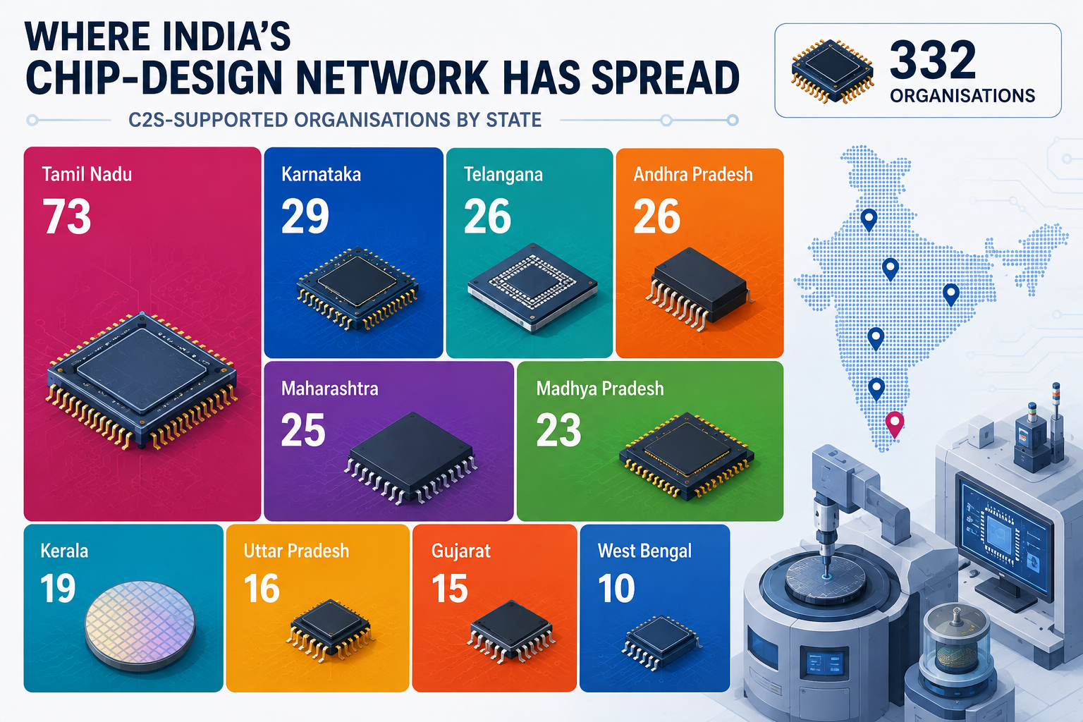
The C2S network now spans hundreds of institutions, including state universities, women’s engineering colleges and campuses in cities and regions that have rarely figured in India’s semiconductor story. The effect is to widen the country’s chip-design base beyond the handful of institutions that dominated it for most of the past three decades.
From access to actual chip design
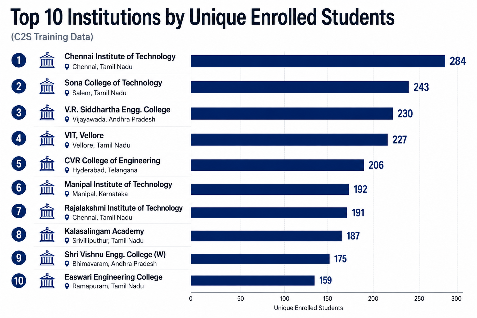
Access to professional design software is only the beginning. C2S has created a much wider training pipeline, bringing students from a far larger pool of engineering colleges into semiconductor design. And the institutional spread is revealing: some of the most active colleges are not the names traditionally associated with India's chip ecosystem. Across its training programme, 22,216 students have enrolled to date, spread over 332 private institutions and six are government.
That matters because semiconductor capability is ultimately built by people who know how to take a design through its entire lifecycle, not simply students who have learnt the theory or used a simulator.
The real test begins when a design has to leave the computer.
The difficult step is tape-out
In chip design, there is a fundamental difference between designing something that works in simulation and sending that design to a foundry for manufacture.
The latter is the point of tape-out. Once a design reaches this stage, it is prepared for fabrication. Errors are no longer corrected by simply running the simulation again. A mistake can mean a failed chip run, wasted time and significant cost. This is where the C2S programme becomes more consequential.
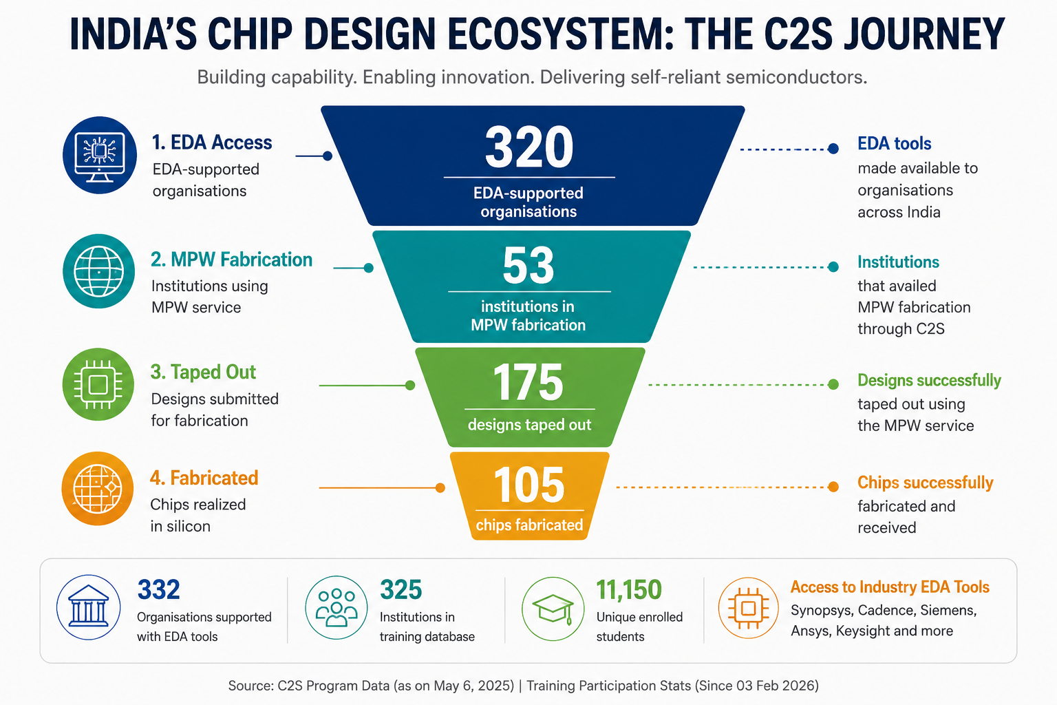
Through Multi-Project Wafer runs, multiple designs can share a wafer fabrication run. For academic institutions and student teams, this creates an opportunity that would otherwise be prohibitively expensive: taking a design developed in a college laboratory and having it manufactured as actual silicon.
The C2S network has already begun moving institutions through this pipeline, from access and training to design, tape-out and fabrication. Of the 332 institutions, 53 have gone on to participate in Multi-Project Wafer.
That progression is more important than the raw number of licences or enrolments.
A programme can distribute software to hundreds of classrooms. It is much harder to produce designs that survive the journey from a computer screen to a foundry.
What students are designing
The designs emerging from the programme also offer a glimpse of where this new talent pool is heading.
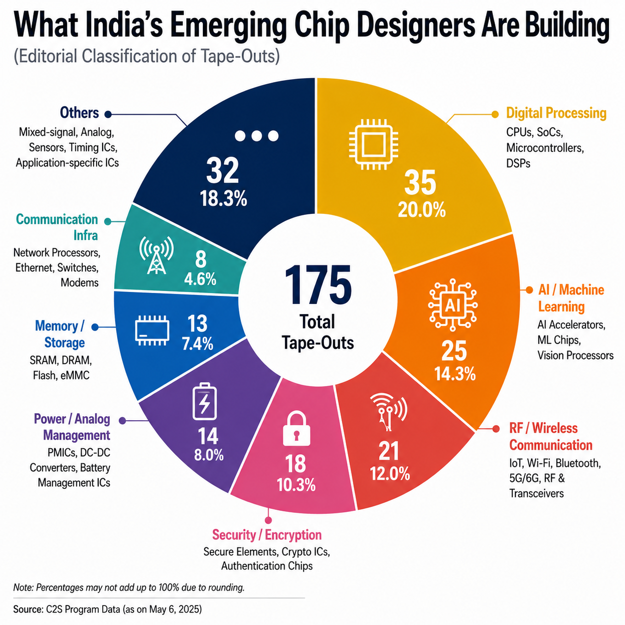
Analogue and mixed-signal work forms a substantial part of the portfolio, including signal-processing blocks, amplifiers, filters and converters, the building blocks that sit inside countless electronic systems.
At the same time, student teams are working on areas at the centre of the global semiconductor race, including AI accelerators and RISC-V processor cores. There is also a smaller but significant stream of security-oriented designs, including encryption-related circuits and an e-passport chip.
The point is not that student projects are about to replace commercial semiconductor design. They are not.
The significance is that students who previously encountered chip design largely as a subject in a classroom are getting an opportunity to experience the entire chain: design, verification, tape-out and, in some cases, working silicon. That is a very different kind of learning.
The geography is changing
The most interesting change may therefore be geographical rather than numerical.
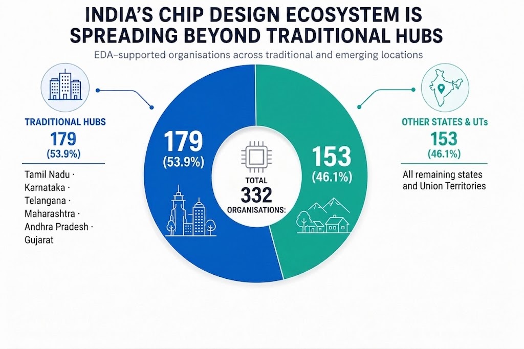
India's semiconductor story has traditionally been concentrated around a familiar group of states. Bengaluru, Hyderabad, Chennai, Pune and other established technology centres have the companies, research institutions, engineering talent and industrial infrastructure that make them natural semiconductor hubs.
C2S has not overturned that geography. The traditional hubs still dominate. But it has begun to create a second layer beneath them.
Institutions in states and regions that would once have been considered peripheral to semiconductor design are now entering the pipeline. Bihar, Odisha, Assam, Jammu & Kashmir, Himachal Pradesh, Punjab and parts of the Northeast are no longer absent from the map.
Their presence should not be exaggerated: the numbers remain much smaller than those of the established hubs. But that is precisely why the change is worth noticing.
The story is not that every state in India has suddenly become a chip-design centre. The story is that the number of places capable of participating in chip design is expanding.
From semiconductor hubs to a semiconductor network
This distinction is important for India's larger semiconductor ambitions.
Much of the public discussion around semiconductors understandably focuses on fabs, packaging plants, investment commitments and billion-dollar projects. Those are the visible parts of the ecosystem.
But a semiconductor industry also needs something less visible: a large and continuously replenished pool of designers, verification engineers and researchers who understand how to build chips.
That talent cannot be created overnight when a fab opens. It has to be cultivated years earlier be it in classrooms, laboratories and engineering projects. This is where C2S may have its most enduring impact.